 |
The Makings of the
Printed Circuit Board (PCB)
These complete instructions on making the PCB is how I made mine. There are many ways to make PCB's now-a-days, but if you would prefer to go a very inexpensive route (or maybe you have never made a PCB before, this method would be a great way to learn using 'Dry Transfers' that can be purchased also at your local Radio Shack store. ), and yet very accurate, the below layout will indeed suffice. From beginning to end, these step-by-step procedures will get you on your way to warm up that soldering iron when the time comes for soldering all of the components on the 'finished' PCB. Let's us begin:
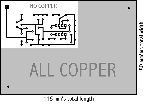
The first picture below is the PCB template. Print out this drawing first. It should come out exactly like the posted measurements. Measure it to be sure it is, in fact, 116 mm's by 80 mm's. If not exact, send the document to a Paint or Graphics Program and stretch or sqeeze to adjust for said measurements. This is extremely important. Make sure the measurements (length and width) are no more 'off' then 1 mm. Once this is done, print out the correct dimensions. Then take a pair of scizzors and cut out the 116 mm's by 80 mm's printed-out template.
Drawing #1
|
Once you have done that, cut out a length and width of 116 mm's by 80 mm's, from a double-sided new PCB. Buff both front and back sides with fine steel wool. A little pressure is needed here to ensure the top layer oxidation residue has been removed. Now place your PCB on the workbench and place the PCB template directly over it, making sure they are both evenly matched up...they should be, if you scizzored-out the PCB template to the correct size as the 'newly-cut' PCB. Tape it all down for it not to move freely. Put the tape around the edges of the PCB template, carefully not covering up any of the circuitry routing. Then proceed to the next step.
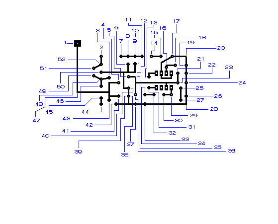
Next, comes the use of a light hammer and center-punch, with a sharp point (or you can use a sharpened-nail). You will be making 52 center-punch 'taps' with your hammer and center-punch. Look at the Drawing #2. This is a blow-up section of the circuitry in Drawing #1. Notice the 'tiny' white dots that are numbered one to fifty-two. These are the exact places (on the 'tiny' white dot) you will put a light tap with the center-punch to form a tiny indentation on the PCB itself. I would suggest you take a scrap piece of PCB and make a few 'different' pressure hits in order to know just how hard you need to hit the center-punch to form an indentation on the PCB. The indentation should be noticeable to the naked eye...these 52 indentations will be your guide as where to place the 'Dry Transfers' later. So make all of the indentations now, making sure each one is a 'good' hit. That way, when it comes time to take off the PCB template, you will see your '52' indentations on the PCB iself. Then take your drill and referring to Drawing #1, drill eight holes (1/32 of an inch drill bit), where the 'low-profile' insert for the LM386 will go. Then drill two more holes for the mounts. These are at the corners...diagonally facing each other. Do this and when you are thru, proceed to the next step.
Drawing #2
 |
The picture below is what your PCB should look like now. All you should be able to see is 52 tiny indentations on the board, plus the eight holes for the LM386 insert and the two mounting holes. It would be a good idea to count all of your indentations to be sure you have not missed any. When you are through with this visual look, proceed to the next step.
Drawing #3
 |
Next, take your Dry Transfers. There are 4 different size 'black-circles' on the transfers. Use the 'second-the-largest' black circles. You will be using 44 of the black circles from the Dry Transfer sheets. Once you have placed them on the PCB (if you have never used Dry Transfers before, look at the accompanying instructions that come in the package for further information on how to place them on the PCB), the below picture should now look exactly like your PCB. After a visual inspeciton and everything looks alright, proceed to the next section.
Drawing #4
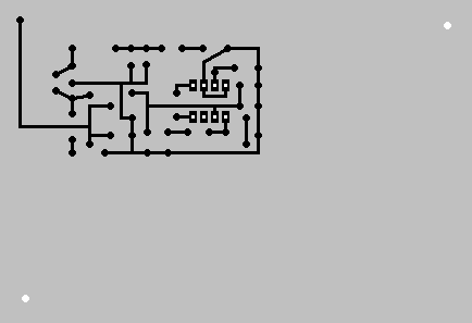
Next on the list will be placement of the Dry Transfer routing. These will be the narrow long straight black lines on the edge of the Dry Transfer sheets. Do not use the larger line, use the narrowest ones you see. There should be around 6 to 8 of them on each sheet of transfers. By referring to Drawing #1, the Template, make all the routes that go to each individual component. As you go through making each individual route, check back with the Template to make sure you have done it correctly. Once all this is through, your PCB should look like Drawing #5, which is below. Begin the next section when you have finished this.
Drawing #5
 |
In this section you will do 2 things:
| Expand the antenna terminal to 1/4 of an inch square |
| Using duct tape, covering top side of PCB where needed |
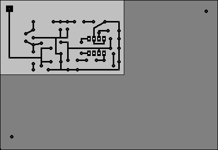
Drawing #6, below, is what the PCB should look like after you have done these two things. Notice where the soldering area is on the antenna terminal (in Drawing #5). In Drawing #6 you have increase the size to one quarter of an inch square. This will be good when placing your wire for the antenna. The larger surface makes it easy to hold the wire. Then you will use duct tape (that two inch wide grey looking tape that you can pick up at a local hardware store) to cover ALL of the topside of the PCB, except 1/8 of an inch from the electrical routing. Look at the drawing below to understand where the tape is to be put. The 'dark' grey area is where the duct tape is applied. The 'light' grey area is where no tape goes. Use a single-edged razor blade to trim off loose threads of tape along the edges of the PCB. Once you have done that correctly, proceed to the next section.
Drawing #6
 |
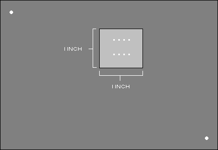
Now we come to the flip side of the PCB. The underneath side of the double-sided PCB should be all copper, except for a one inch square that will surround the LM386 chip. Drawing #7 will give you a guide as to how the one inch square is positioned. Put your duct tape on the 'dark' grey area of the picture below. Do not put tape on the 'light' grey area on the picture below. Try and center the one inch square so that when it comes time to put the LM386 in place, it will be right in the center of the square.
Drawing 7
 |
You have just finalized the PCB before putting it into the echant solution. Take a break now and re-inspect both sides of the PCB to make sure everything was done right. If you have never used echant solution before, do this: Find yourself a glass or plastic tray that the PCB will fit into. Then pour about 1/4 of an inch of echant solution into the tray. Put the PCB into the solution. Rock the tray every 10 seconds or so until all of the copper is removed from the 'untaped' areas in the circuitry routing. When all of the copper is then removed, flip the PCB over to make sure the one inch square of copper has been removed too. Total time will run around 20 minutes or so...give or take a few minutes for differences in temperature. Once all of the copper has been removed, wash the board in regular tap water and remove the duct tape...again wash it some more...about 3 minutes or so...making suring fresh water gets into the 10 drilled holes. Then dry it and take your fine steel wool and remove all of the black 'dry transfers' that are still on the board. All of the copper, frontside and back, plus the electrical routing will be shiny and new once you have brushed it up with your steel wool...
Well, my friend, that's about it...go back to the Radio Shack Special Page and continue the project, as we shall begin to solder the components to the 'finished' and now ready...PCB!
Patrick's Email
address
Patrick's
Home Page with the new version of this project